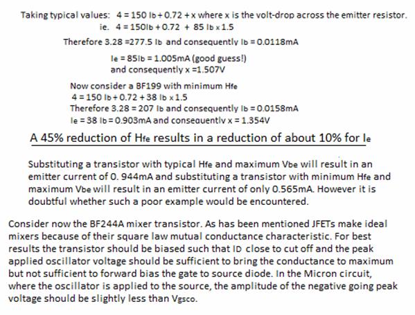
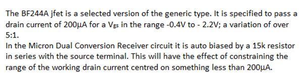
Norcim rc electronics club page 15……
![]()
![]()
![]()
TRANSISTORS AS AMPLIFIERS BY DAVID CAUDREY
BEFORE THE JUNCTION TRANSISTOR
Young electronics engineers are often astonished to learn that transistors existed before the junction types which are in universal use nowadays. Shortly before the establishment of the Germanium junction transistor, point contact transistors were developed and marketed in the US and the UK. Basically these devices had similar characteristics to junction transistors but with some significant differences. These differences were both advantageous and disadvantageous according to application:-
 The
most significant difference between the types was that point contact
transistors were capable of producing current gain when operated in the common
base configuration. Thus the collector current could be up to five times the
emitter current although a more typical value would be around 2.5 times.
The
most significant difference between the types was that point contact
transistors were capable of producing current gain when operated in the common
base configuration. Thus the collector current could be up to five times the
emitter current although a more typical value would be around 2.5 times.
On the plus side this enabled very simple oscillator circuits to be constructed but on the minus side precautions had to be taken to prevent oscillation in amplifier circuits.
Another plus was that the inter-electrode capacities of point contact transistors were typically much smaller than those of junction transistors due to the smaller ‘junction’ areas of the former. This, coupled with lower base resistance, enabled point contact transistors to operate at much higher frequencies than the junction types then current. Point contact transistors capable of operating up to 100MHz were available when junction transistors were struggling to operate at 100kHz.
Ultimately the junction types won out, possibly because they were more rugged and easier to manufacture and to use. This, coupled with a potential for development of high frequency junction devices probably settled the fate of point contact transistors before 1960.
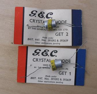
The point contact transistors pictured were developed by the Hirst Research Centre of GEC about 1947 and were given to the author by an engineer who was studying the possibility of their use as thermionic valve replacements in hearing aids. Unfortunately neither is functional now despite being kept in their sealed packaging until a couple of years ago.
NOW ON TO BIPOLAR TRANSISTORS
With the wide availability of operational amplifiers the design of amplifiers using discrete component transistors is not widely practiced nowadays but, if low noise and a degree of flexibility are required, a discrete component amplifier will have advantages over its integrated equivalent
The following details the author’s method for using transistors in amplifiers. Initially it attempts to show how the bipolar transistor may be conveniently treated as a voltage driven device permitting direct comparison with field effect transistors and thermionic valves.
For the purpose of this study it is necessary to state the following: -
1) A transistor operating in common emitter or common collector mode is not driven by a signal current flowing into the base terminal.
2) A silicon transistor does not need 0.6V between the base and emitter terminal to ‘turn it on’ – there is no threshold.
3) The voltage between emitter and base causes a current to flow into the emitter.
4) The
current carriers which constitute the emitter current drift by field attraction
across the reverse-biased base to collector diode. In this action a small
proportion of them recombine in the base region and it is this loss which
constitutes the base current. Ideally the proportion of carriers which
recombine should be zero or very small and constant. For a typical modern small
signal transistor the proportion of emitter current carriers which recombine in
the base region is between 0.1% and 0.5%; defining hfe
values between 1000 and 200. Base current is therefore purely
accidental and consequently hfe is not
strictly a characteristic but is simply a parameter for 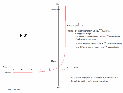 an individual transistor.
5) Discounting frequency range and power handling capability, all bipolar transistors are identical and will give exactly the same voltage gain at the same emitter current.
All transistors passing an emitter current of 1mA will have a mutual conductance (dIc/dVbe) of approximately 40mA/V at room temperature or, expressed another way, have a 25Ω resistor in series with the emitter terminal. At an emitter current of 100µA the corresponding figures will be 4mA/V and 250Ω respectively.
Knowledge of items 2) and 5) above is all one needs to commence the basic design of amplifiers which embody bipolar transistors. Of course transistors have other parameters such as internal negative feedback due modulation of the depletion depth of the reverse biased base to collector diode due to variation of the collector
voltage and the conductance shunting the base to collector diode. However these are small in effect and do not significantly affect amplifier design or a facility to assess at a glance the open loop gain of an amplifier circuit.
The aim of the following is to justify these claims from the diode characteristic:
 From the above FIG 1 (and the material
left) it can be seen that at a given current the emitter to base diode has an
effective series resistance (re) which is inversely dependent upon the
magnitude of the current passed by the diode. The resistance of the connections
to the junction must be taken into account but these are usually small in
comparison with 25Ω.
From the above FIG 1 (and the material
left) it can be seen that at a given current the emitter to base diode has an
effective series resistance (re) which is inversely dependent upon the
magnitude of the current passed by the diode. The resistance of the connections
to the junction must be taken into account but these are usually small in
comparison with 25Ω.
A signal which modulates Vbe will obviously modulate Ie and cause re to vary. Therefore an amplifier which produces gain by virtue of transistor action (causing Ie, and variations thereof, to flow through a much larger external resistor in the collector circuit) will be subject to gross distortion unless the signal voltage is very small.
For a transistor passing a collector current of 1mA and operating from a 10V supply a collector load resistance of 4.7k will result in a collector voltage of about 5V (the condition for maximum output). With no additional resistance in the emitter circuit, the potential small signal voltage gain for this transistor is 4700/25 = 188 However distortion and bandwidth considerations make it advantageous to obtain high gain by two or more stages of moderate gain which may be effected by adding external resistance to re.
Used as a common base amplifier at a prescribed emitter current less than 1mA, re can be set to match the impedance of a coaxial cable for maximum power transfer – a useful feature in the design of radio frequency amplifiers.
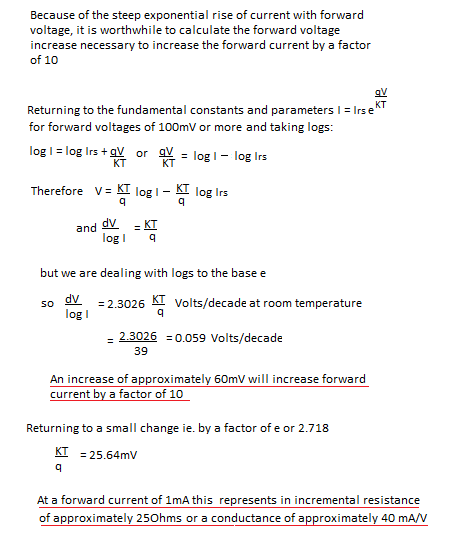
Biasing a Transistor for a Given Collector current.
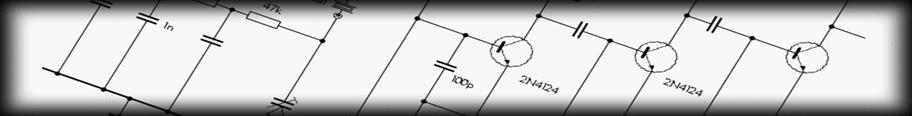
In the early days of transistors, transistors operating in common emitter circuits were often biased by a single resistor between the base and the collector supply to determine the base current. Thus the emitter current was dependent upon the widely variable Hfe. Emitter current also increased with temperature and germanium transistors were prone to destruction due to thermal runaway. The solution to these difficulties is to voltage bias a transistor using a potentiometer as shown below. Thermal stability is also enhanced by adding a resistor in the emitter circuit. This resistor may be used un-decoupled to define a lower voltage gain or wholly or partially decoupled by a capacitor to produce a higher gain at signal frequency. Consider the circuit to the right. FIG 2.
 From
the circuit it can be seen that the collector voltage is approximately half of
the supply voltage which permits the largest peak to peak ac output voltage
excursion. As depicted the circuit will have a voltage gain of 4.7/1.8 = 2.6
and the input resistance at the transistor base will be approximately 1.8 x Hfe k = 126 to 540k.
From
the circuit it can be seen that the collector voltage is approximately half of
the supply voltage which permits the largest peak to peak ac output voltage
excursion. As depicted the circuit will have a voltage gain of 4.7/1.8 = 2.6
and the input resistance at the transistor base will be approximately 1.8 x Hfe k = 126 to 540k.
If the 1.8k resistor is bypassed by a suitable capacitor the circuit will have an ac. gain of approximately 188 and an input resistance of 1.75 to 7.5k dependent upon Hfe. The 1.8k resistor may be made up from two resistors totalling 1.8k and by bypassing one of these with a suitable capacitor, any voltage gain from 2.6 to 188 may be attained.
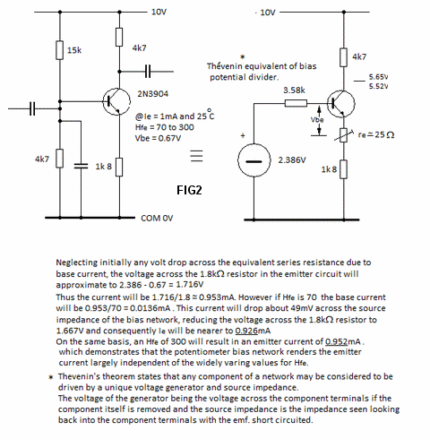
 Sharp
eyed readers will notice that the capacitor which decouples the bias network to
common also decouples the signal and it is therefore necessary to add a
resistor between the network and the base terminal as shown in FIG 3 in a
practical circuit. This will reduce emitter current significantly unless a
transistor with a typically high value of Hfe (BC109
for example) is used.
Sharp
eyed readers will notice that the capacitor which decouples the bias network to
common also decouples the signal and it is therefore necessary to add a
resistor between the network and the base terminal as shown in FIG 3 in a
practical circuit. This will reduce emitter current significantly unless a
transistor with a typically high value of Hfe (BC109
for example) is used.
From the foregoing, this amplifier would be expected to have a gain of 10 with equal input and output impedances of 4.7k
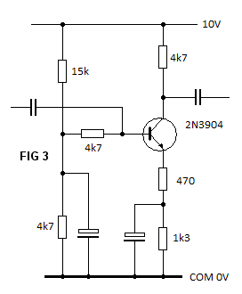
For a further example of transistor biasing consider the direct coupled ‘ring of three’ amplifier circuit (see FIG 4) in which each transistor is arranged to bias its fellow. The amplifier comprises two amplifier stages VT1 and VT2 and an emitter follower output stage VT3. Each of the amplifier stages have a gain of approximately 10 (re for VT1 will be approximately 250Ω giving a total gain of about 100 before the application of feedback.
In this circuit the open ac. loop gain
may by increased by capacitive decoupling part or all of the emitter resistors
of either VT1 or VT2. However in the former case it would be necessary to
change the feedback 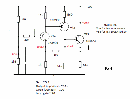 resistor to maintain an ac gain of about five.
Without feedback the output impedance of the emitter follower VT3 would be re ie. about 25Ω With feedback this is divided by the loop gain.
A problem with such amplifiers is that they are susceptible to disturbances of the supply rails (poor common mode rejection ratio CMRR) and change of temperature. With regard to the latter, Vbe falls by 2 to 2.5mV for every degree rise of temperature.
Note. For the mathematically inclined dVbe/dt does not fall out directly from the diode equation above because the temperature dependence of Irs must be taken into account.
 The solution to poor CMRR and
temperature dependence is the long tailed pair differential amplifier which is
found consequently in almost all operational amplifiers.
The solution to poor CMRR and
temperature dependence is the long tailed pair differential amplifier which is
found consequently in almost all operational amplifiers.
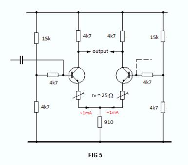
The example shown in FIG 5 is a combination of the original circuit and a mirror image of itself. For the best CMRR and independence from the effects of temperature change, the output signal is taken from both collectors, the voltage at one rising as the voltage at the other falls. In this differential mode of operation there is no need to decouple the bias networks because movements of the supply rails have no effect upon the differential output. Similarly there is no need to decouple all or part of the common 910Ω resistor. In fact, unlike the single ended circuit, the common resistor pays no part whatsoever in determining the gain and can be replaced by a 2mA constant current source if desired.
The differential gain for a small signal will be the same as that for the single ended circuit ie. approximately 188 and the gain for the signal at each collector individually is thus 94. This because each of the transistors has effectively two times re. (50Ω) in series with its emitter. If it is required to reduce the gain of the amplifier, separate resistors must be connected between the transistor emitter terminals and the commoning resistor.
JUNCTION FIELD EFFECT TRANSISTORS AS AMPLIFIERS
When junction gate field effect transistors came on the scene in the early 1960s engineers who had cut their teeth on thermionic valves were encouraged by the realization of what was effectively a low voltage valve with the added bonus of the availability valves of reverse polarity. Having high input impedance with mutual conductance and ‘negative’ gate control voltage characteristics similar to valve, they permitted familiar stock formulae for rf. circuits to be dusted off. However there was a pitfall because unlike bipolar transistors the basic parameters of field effect transistors vary dramatically from one to another; sometimes by a factor of ten or more as typified by the general purpose 2N3819 and the complementary 2N3820 JFETs. This wide variation makes it difficult to design amplifier circuits without the need to incorporate trimmers or select the devices.
However JFETs have advantages which far outweigh the disadvantages for some applications.
As will be seen the relationship between the drain current and the gate to source is a square law function which makes them ideal for use as mixers in radio receivers, giving high conversion conductance and lower noise and distortion than their bipolar counterparts. Also because of their low input (gate) current and the presence of only one junction they produce very low noise levels and consequently an fet input stage is essential for a low noise wideband amplifier. [Paradoxically mosfets., with even lower gate currents, are noisy devices, particularly at low frequencies, but they are not within the scope of this note]. Shown in F are the characteristics of a typical general purpose JFET.
The left hand curve (red) shows the relationship between drain current and gate to source voltage for a fixed drain to source voltage. This typifies the best of a given type; a poorer example of the same might be represented by the orange curve.
The right hand curves show the relationship between drain current and drain to source voltage with gate to source voltages as parameters.
In a field effect transistor the magnitude of the drain current is influenced by the combination of the transverse field produced by Vgs and the longitudinal field produced by VDS.
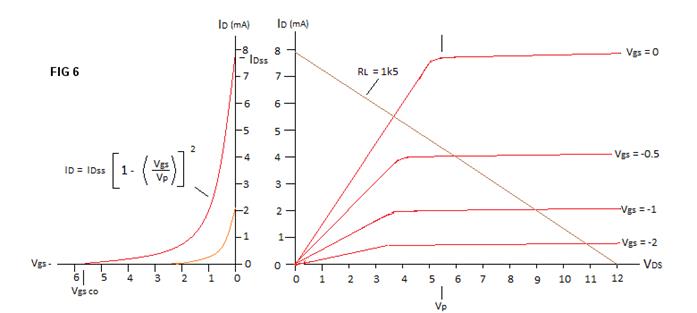 The
combination of the fields due to the sum of Vgs and
VDS ‘pinches’ the conduction channel the restricting drain current. When this
sum exceeds a certain voltage (Vp)
the current will not increase if VDS is increased further and the channel is
said to be pinched off. In the right hand family of curves pinch off is the
locus of the ‘knees’ of the individual curves.
The
combination of the fields due to the sum of Vgs and
VDS ‘pinches’ the conduction channel the restricting drain current. When this
sum exceeds a certain voltage (Vp)
the current will not increase if VDS is increased further and the channel is
said to be pinched off. In the right hand family of curves pinch off is the
locus of the ‘knees’ of the individual curves.
For the curve Vgs = 0 the knee occurs at a
drain to source voltage of about 5.5V and thus Vp for the transistor is about 5.5V. In the left hand red curve there is zero drain current when Vgs = - 5.5V. This is known as the cut-off voltage (Vgsco) and it is apparent that Vgsco = Vp.
Referring to the left hand red curve the mutual conductance gfs is given by the slope dID/dVgs and by inspection this can be seen to be something like 5mA/V at a drain current of 5mA. Or, expressed as a resistor in series with the source terminal, rs = 200Ω. For comparison a bipolar transistor operating at a collector current of 5mA would have a mutual conductance of 200mA/V and or a corresponding re of 5Ω.
Biasing
a Junction Field Effect Transistor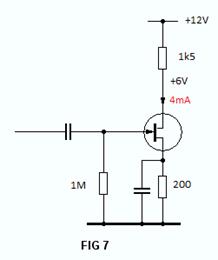
Because the gate terminal is normally at a negative potential with respect to the source terminal, a JFET can be biased by a single resistor in series with the source terminal if the gate is referred to common ground.
Referring to the left hand curve it can be seen that Vgs for a drain current of 4mA is about -0.5V. If a 200Ω resistor is connected in series with the source terminal 0.5V will be dropped across it if the current through the transistor channel is 4mA and the gate terminal is therefore 0.5V negative of the source to meet the bias condition. Operating from a 12V supply a drain voltage of half the supply voltage will be produced by a 1.5k drain resistor.
With
a drain load of this value, the voltage gain is given by gfs RDL or RDL/rs = 7.5 provided
that the 200Ω source 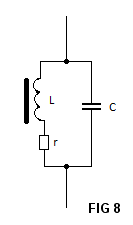 resistor is decoupled by a suitable
capacitor as shown in FIG 7. A 1.5k load line is shown superimposed on the
right hand curves. This shows that the amplifier response would not be linear
for other than very small input signals and that, should the gate be driven
positive by a small amount, the transistor is not pinched off and consequently
the CMMR will be impaired. Not a good amplifier design but it serves to
illustrate the problems of designing with JFETs.
resistor is decoupled by a suitable
capacitor as shown in FIG 7. A 1.5k load line is shown superimposed on the
right hand curves. This shows that the amplifier response would not be linear
for other than very small input signals and that, should the gate be driven
positive by a small amount, the transistor is not pinched off and consequently
the CMMR will be impaired. Not a good amplifier design but it serves to
illustrate the problems of designing with JFETs.
As mentioned the non-linearity of junction field effect transistors is advantageous with regard to their use in rf. mixer circuits where a received signal and a local oscillator signal are applied to the gate terminal and the drain load is a circuit tuned to the difference frequency. Alternatively one of the inputs can be applied to the gate and one to the source.
For these applications the drain load is usually a parallel tuned circuit: (FIG 8)
To find the gain of an amplifier which has a resonant parallel tuned circuit as a load, it is necessary to know the equivalent resistance presented by the circuit; known as the dynamic resistance Rd. Rd is given by L/Cr or ωLQ where ω = 2πf and Q = the resonant frequency divided by the -3dB bandwidth.
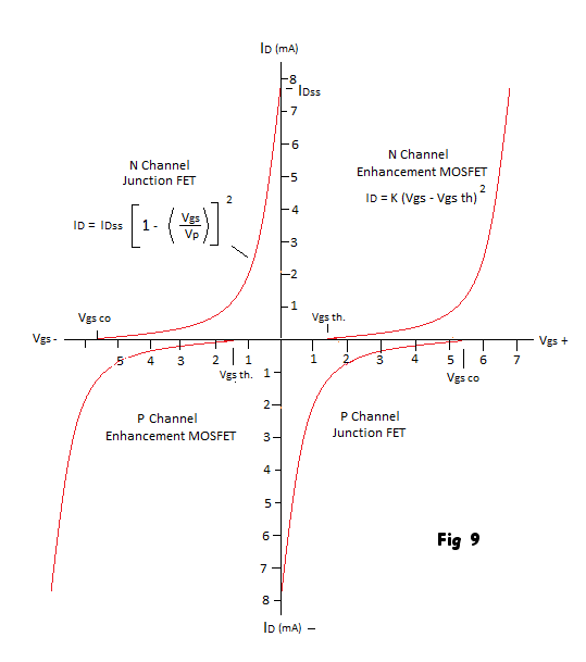 For completeness Figure 9 shows combined mutual
conductance characteristics typical of the four main types of field effect
transistor. MOSfet transistors generally
operate in the enhancement mode with characteristics as shown. However
depletion mode MOSfets are used for some radio
frequency applications. These have characteristics similar to Jfets.
For completeness Figure 9 shows combined mutual
conductance characteristics typical of the four main types of field effect
transistor. MOSfet transistors generally
operate in the enhancement mode with characteristics as shown. However
depletion mode MOSfets are used for some radio
frequency applications. These have characteristics similar to Jfets.
Because of their low gate current Jfets are low noise devices compared to bipolar transistor and consequently they ideally ideally suited for use in audio and instrument amplifiers. MOSfets have even lower gate currents but paradoxically they are very noisy at low frequencies. This is because the gate terminal is insulated from the Source-Drain channel by a very thin layer of silicon oxide or nitride and sometimes both. Such thin layers are subject to what is termed micro plasma breakdown which results in ‘popcorn’ noise; so called because of how it sounds in the output signal of an audio amplifier. This noise per unit bandwidth diminishes rapidly with increasing frequency and consequently MOSfets are widely used in radio frequency amplifiers and logic circuits.
Many MOSfets are symmetrical and consequentially either channel terminal may be used as the drain or source. This facility is employed in the ‘Zero Drop Diode’ on Page 10 of these Notes.
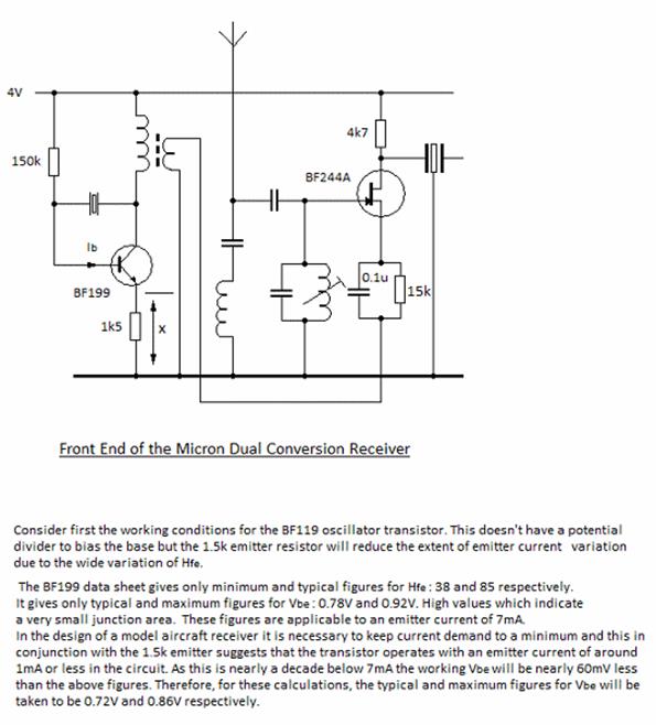
An Example of Practical Application
The front end of the Micron Dual Conversion Receiver embodies a bipolar transistor operating as the first local oscillator and a JFET operating as the first mixer.
The Bipolar Transistor as a Bandgap Voltage Reference
The voltage reference in semiconductor circuits is usually termed a Zener diode; examples of which can be obtained to produce voltages ranging from about 1.5V to 300V.
In fact the Zener effect applies only to voltages below about 5V and above which the avalanche effect comes into play; both effects being involved to some extent in diode voltage references below 15V or so.
The Zener effect is characterised by a negative temperature coefficient of voltage and the avalanche effect is characterized by a positive coefficient. At a reference voltage in the region of 5V these coefficients theoretically cancel to produce a zero temperature coefficient but this cannot be relied upon. Precision voltage reference diodes such as the IN825-29 series combine a ‘Zener’ diode with a series forward biased diode to produce a voltage reference of 6.2V with virtually zero temperature coefficient but this is only achieved when passing a current of 7.5mA
Such devices can be integrated into monolithic integrated circuits but clearly they are not suitable for low voltage and low power circuits.
The problem of finding a low voltage-low power temperature independent voltage reference for use in integrated circuits was addressed by an American engineer Robert J Widlar who consequently is regarded as the father of the analogue integrated circuit.
The most basic form of his invention is shown in Figure 10. It comprises three identical transistors and three resistors and to understand its operation the reader is asked to accept, for the time being, that the reference voltage produced is 1.2V as shown.
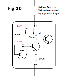 The
transistors in figure 10 are of a small signal variety requiring a VBE of 0.6V
for an emitter current of ImA. If the reference
voltage is 1.2V it is clear that the left hand diode-strapped transistor will
pass a current of 1mA causing 0.6V to be dropped across the 600R series
resistor. With a 6K series resistor the centre
transistor can only pass 100microA and as discussed earlier its VBE will be 60mV
less, ie. 0.54V, with the 60mV deficit dropped across
the 600R resistor in series with its emitter. The VBE for the left hand
transistor will change by approximately -2mV/oC
rise in temperature and Widlar realized that the
equivalent change of VBE with temperature for the centre
transistor would 10% less. Ie. the
temperature coefficient of ∆VBE is equal but positive.
The
transistors in figure 10 are of a small signal variety requiring a VBE of 0.6V
for an emitter current of ImA. If the reference
voltage is 1.2V it is clear that the left hand diode-strapped transistor will
pass a current of 1mA causing 0.6V to be dropped across the 600R series
resistor. With a 6K series resistor the centre
transistor can only pass 100microA and as discussed earlier its VBE will be 60mV
less, ie. 0.54V, with the 60mV deficit dropped across
the 600R resistor in series with its emitter. The VBE for the left hand
transistor will change by approximately -2mV/oC
rise in temperature and Widlar realized that the
equivalent change of VBE with temperature for the centre
transistor would 10% less. Ie. the
temperature coefficient of ∆VBE is equal but positive.
The centre transistor constitutes an amplifier with a gain of 10 to produce a voltage of -10 x ∆VBE at the collector and which is added to VBE for the left hand transistor by the action of the right and transistor and the ballast resistor. In effect 0.6V with a positive temperature coefficient is added to 0.6V with an equal negative temperature coefficient to produce a voltage reference of 1.2V with zero temperature coefficient. The arrangement of the right hand transistor provides 100% negative feedback; reducing the output impedance.
Why is it called a bandgap reference? It is called a bandgap reference because 1.2V is the energy gap between the valence and conductance bands for silicon at absolute zero temperature. Band gap references are series connected to produce reference voltages of 2.4V, 3.6V etc. as required and are available as discrete ‘diodes’ for incorporation in circuits.
They are used widely in analogue integrated circuits and they are fairly easy to identify in the circuit schematics. However it is probable that those identified will be more complex than the basic arrangement discussed in order to enhance performance.
Another advantage of bandgap references is that they are far less noisy than Zener/avalanche devices. The latter, being dependent upon breakdown, are rich sources of ‘popcorn noise’. The author once used a 15V ‘Zener’ as the noise source for a random pulse generator.
A LOW COST AUDIO AMPLIFIER DESIGN BY ‘DC’. ∆
THE CURRENT MIRROR CIRCUIT
The long tailed pair circuit shown in Figure 5 has in fact a relatively short tail in the form of a 910Ω resistor. A ‘short tail’ reduces the current transfer from one amplifier transistor to its partner and performance would be improved by a longer tail in the form of a larger resistor to a negative supply. Provision of an additional negative supply is not always practicable and the alternative of employing a 2mA ‘constant current’ source in lieu of the 910Ω resistor is worth consideration:
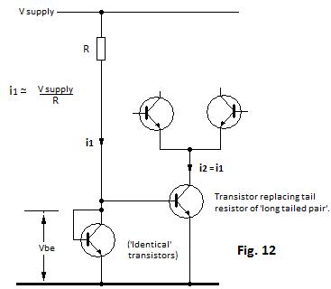 Two
terminal ‘constant current’ sources are available; these are in fact junction fets. with gate and source
terminals connected such that the current passed is IDSS. It appears
that manufacturers select and categorize these
devices. The problem with fet
constant current sources is that they must be pinched off (see the foregoing fet. characteristics) to achieve constant current operation
and that the VDS required to do this can be quite high and vary
significantly from one example to another. It is therefore also worthwhile to
consider the possibility of using a bipolar transistor in lieu of the 910Ω
tail resistor:
Two
terminal ‘constant current’ sources are available; these are in fact junction fets. with gate and source
terminals connected such that the current passed is IDSS. It appears
that manufacturers select and categorize these
devices. The problem with fet
constant current sources is that they must be pinched off (see the foregoing fet. characteristics) to achieve constant current operation
and that the VDS required to do this can be quite high and vary
significantly from one example to another. It is therefore also worthwhile to
consider the possibility of using a bipolar transistor in lieu of the 910Ω
tail resistor:
The collector impedance of a transistor connected in the common emitter configuration is much less than the drain impedance of a pinched off fet., but being typically in the region of 70kΩ, it is much higher than can be attained with practicable resistor tail even with the availability of a negative supply. Also this collector impedance is essentially maintained for very small collector to emitter voltages, permitting operation with a collector to emitter voltage less than the base to emitter voltage needed to produce the required collector current.
Using voltage directly to bias a transistor for given collector current is not practical and the solution is to bias the tail transistor using the current mirror circuit shown in Figure 12.
In this circuit the current passed by the tail transistor mirrors that of its diode-strapped companion; the current through which is determined by a resistor from the supply. Thus it may be set to a required value by selection of a resistor of appropriate value. For mirror operation both transistors must be of the same type and monolithic pairs on a chip give the best results.
Current mirrors are frequently used in operational amplifiers and can easily be identified in the circuit schematics where available.
THE CASCODE AMPLIFIER
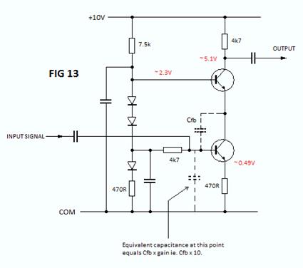 Transistors
are often used in pairs to mitigate the shortcomings of a single
transistor. Figure 13 depicts a simple amplifier intended to produce a
voltage gain of 10 with equal input and output impedances of approximately
4.7kΩ. In this circuit the bottom transistor is the amplifier with the
output signal developed across a 4.7kΩ load resistor in its collector
circuit. However interposed between the collector terminal and the load
resistor is a transistor connected in common base amplifier configuration. The
purpose of this intermediate transistor is to increase the bandwidth of the
amplifier by reducing the effect of the collector to base capacitance of the
amplifying transistor. Without the series transistor this capacitance, labeled Cfb in the schematic, produces increasing negative feedback
with increasing frequency, severely limiting bandwidth. It is usual to model
this effect (known as the Miller effect after the engineer who identified it in
thermionic valve circuits) by an equivalent capacitance across the input
terminals, equal to Cfb x gain. With the interposed
common base stage there is no gain at the collector terminal of the amplifying
transistor (where Cfb is effective) because the
effective load resistance is the input resistance of a common base connected
transistor (about 25Ω in this instance) and consequently the equivalent
input capacitance equals Cfb. However the collector
signal current flows through the common base amplifier to be developed as a
voltage signal across the load resistor. Because the common base amplifier is
non-inverting, with its base terminal held at fixed potential, the capacitance
between collector and base terminals does not produce negative feedback.
Transistors
are often used in pairs to mitigate the shortcomings of a single
transistor. Figure 13 depicts a simple amplifier intended to produce a
voltage gain of 10 with equal input and output impedances of approximately
4.7kΩ. In this circuit the bottom transistor is the amplifier with the
output signal developed across a 4.7kΩ load resistor in its collector
circuit. However interposed between the collector terminal and the load
resistor is a transistor connected in common base amplifier configuration. The
purpose of this intermediate transistor is to increase the bandwidth of the
amplifier by reducing the effect of the collector to base capacitance of the
amplifying transistor. Without the series transistor this capacitance, labeled Cfb in the schematic, produces increasing negative feedback
with increasing frequency, severely limiting bandwidth. It is usual to model
this effect (known as the Miller effect after the engineer who identified it in
thermionic valve circuits) by an equivalent capacitance across the input
terminals, equal to Cfb x gain. With the interposed
common base stage there is no gain at the collector terminal of the amplifying
transistor (where Cfb is effective) because the
effective load resistance is the input resistance of a common base connected
transistor (about 25Ω in this instance) and consequently the equivalent
input capacitance equals Cfb. However the collector
signal current flows through the common base amplifier to be developed as a
voltage signal across the load resistor. Because the common base amplifier is
non-inverting, with its base terminal held at fixed potential, the capacitance
between collector and base terminals does not produce negative feedback.
Another advantage is that the collector output admittance in the common base configuration is much smaller than that for the common emitter configuration so effectively the collector load resistance is minimally shunted by the transistor. An important consideration when a large load resistor is used.
Also in Figure 13 the transistors are biased by a current mirror circuit such that the quiescent collector current of the transistors is approximately equal to the current flowing through the resistor-diode bias chain.
THE WHITE EMITTER FOLLOWER
Figure 14
depicts a two transistor White emitter follower circuit which overcomes problems
of the conventional emitter follower, particularly when driving larger
amplitude signals into a capacitive load. 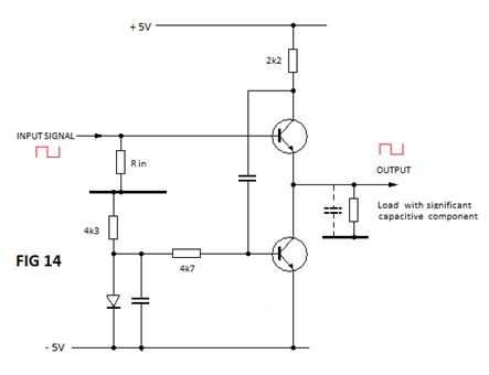
For low amplitude signals, the simple emitter follower circuit is characterised by high input impedance and low output impedance. It can drive low impedance loads with a gain close to unity. However for larger (particularly pulse) signals the negative going excursions of a signal are distorted because of the transistors inability to draw current from the load capacitance when turning off. The emitter follower thus exhibits a poor slewing rate for negative going signal excursions.
In figure 14 positive and negative supplies are employed to facilitate negative excursions of a direct-coupled signal relative to common zero. The upper transistor is the emitter follower and the lower transistor acts as a constant current 1mA source defining the quiescent current for both transistors.
Unlike a normal emitter follower the upper transistor has a resistor in its collector circuit. Normally a resistor in this position would impair performance to some degree but in this case it facilitates capacitive feedback to the base of the lower transistor which greatly enhances performance. The effect of the feedback is to turn off current from the lower transistor during positive transitions of the signal. This assists the upper transistor to a small extent but it is well capable of driving of driving current into the load in any case. However during negative excursions the action of the feedback is to drive the lower transistor into increased conduction such that it sinks current from load capacitance, dramatically improving the slewing rate.
In fact the feedback greatly reduces the high frequency output impedance relative to a simple emitter follower for small as well as larger signals (up to about 60 times in this instance) so both bandwidth and slewing rate are improved by the White emitter follower circuit.
David Caudrey